Applications
Since the rising of the electronic and nanoscience era, the miniaturization of electronic components has become an essential factor in their almost-exponential performance. The thinning of technical layers and coatings down to nanometric scales allow advances in a varied range of fields. Sophisticated manufacturing processes drive controls to be increasingly accurate.
NETA provides solutions to many problematics related to these evolutions. The detection of defects is now essential in many industries to avoid problems encountered during production and to improve the level of quality.
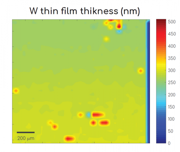
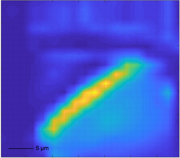
The JAX technology is effective on a wide range of materials
The large range of materials and their use in many applications make this material aspect essential. Since Neta's inception, our technology has proven its capability to measure many metallic material.
It is this experience that we want to offer to our customers. JAX is also suitable for ceramics and metal oxides and is free from form factors.
Non-Destructive Testing (NDT) finds its utility in a wide range of applications
The semiconductor industry
The semiconductor industry provides the basic component for most of the electronic devices we encounter around us. Today it is an essential component for the deployment of all electronic solutions of our knowledge. Its manufacture requires multiple thin film deposits on silicon wafers.
Problematics? As in any industrial process, the deposition of opaque thin films, whether single or multilayer, requires quality control. Whether in inspection or in metrology, thickness measurement and interface characterization are crucial issues to ensure their quality.
Our solutions?
- High-speed control.
- Non-destructive and contactless measurement.
- Single and multilayer thickness measurement.
The displays industry
Different technologies compete today to dominate the production of displays, which are everywhere in our daily use. Indeed, this expanding industry has technical constraints due to manufacturing processes for future UHD-8K standards as well as for emerging flexible displays.
Problematics? A pixel remains a stack of thin layers of organic inks, silver, ITO... In this regard, the issues of controlling the thickness of thin layers remain. These issues can then lead to quality defects on the final product.
Our solutions?
- Unique inspection of this type of layer.
- Possibility of extracting thicknesses.
- Non-destructive and contactless thickness measurement.

Thin Layer Deposition
Whether it is in the aeronautics industry or for the manufacturing of medical devices, technical coatings can be used to reinforce some functions in high value-added components. The thickness of these coatings then becomes a critical factor to ensure the targeted performances.
Problematics? Whether it be for legal or technical constraints, sampling methods with destructive testing often provides incomplete answers. In addition, it is difficult to control 3D pieces because of their shape factors, curvature, etc.
Our solutions?
- Form factor postage
- Non-destructive and contactless testing
- Quick access to thickness data
- On-line production control now possible